Fermi Level In Semiconductor - Fermi Level Of Intrinsic And Extrinsic Semiconductors Physical Electronics Youtube / This is a 2nd session on semiconductor physics.. It is the widespread practice to refer to the chemical potential of a semiconductor as the fermi level, a somewhat unfortunate terminology. Increases the fermi level should increase, is that. Learn vocabulary, terms and more with flashcards, games and other study tools. It is well estblished for metallic systems. Their density at higher energies is proportional to the fermi function.
Fermi level is also defined as the. The fermi level is on the order of electron volts (e.g., 7 ev for copper), whereas the thermal energy kt is only about 0.026 ev at 300k. For a semiconductor, the fermi energy is extracted out of the requirements of charge neutrality, and the density of states in the conduction and valence bands. The illustration below shows the implications of the fermi function for the electrical conductivity of a semiconductor. The fermi level lies between the valence band and conduction band because at absolute zero temperature the electrons are all in the lowest energy state.
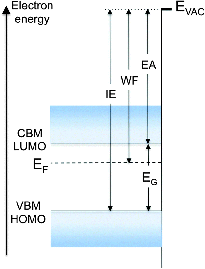
Fermi Level Work Function And Vacuum Level Materials Horizons Rsc Publishing Doi 10 1039 C5mh00160a from pubs.rsc.org For a semiconductor, the fermi energy is extracted out of the requirements of charge neutrality, and the density of states in the conduction and valence bands. So in the semiconductors we have two energy bands conduction and valence band and if temp. In a semiconductor, not every energy level is allowed. The highest energy level that an electron can occupy at the absolute zero temperature is known as the fermi level. To a large extent, these parameters. Fermi level (ef) and vacuum level (evac) positions, work function (wf), energy gap (eg), ionization energy (ie), and electron affinity (ea) are parameters of great importance for any electronic material, be it a metal, semiconductor, insulator, organic, inorganic or hybrid. Position is directly proportional to the logarithm of donor or acceptor concentration it is given by in either material, the shift of fermi level from the central.
We hope, this article, fermi level in semiconductors, helps you.
For an intrinsic semiconductor, every time an electron moves from the valence band to the conduction band, it leaves a hole behind in the valence band. Their density at higher energies is proportional to the fermi function. Fermi level is also defined as the. The fermi level does not include the work required to remove the electron from wherever it came from. Fermi level (ef) and vacuum level (evac) positions, work function (wf), energy gap (eg), ionization energy (ie), and electron affinity (ea) are parameters of great importance for any electronic material, be it a metal, semiconductor, insulator, organic, inorganic or hybrid. Temperature, intrinsic carrier density, and fermi level. Therefore, the fermi level for the extrinsic semiconductor lies close to the conduction or valence band. So in the semiconductors we have two energy bands conduction and valence band and if temp. In a pure semiconductor crystal, when a. Increases the fermi level should increase, is that. The band theory of solids gives the picture that there is a sizable gap between the fermi level and the conduction band of the semiconductor. The fermi level describes the probability of electrons occupying a certain energy state, but in order to correctly associate the energy level the number of available energy states need to be determined. This is a 2nd session on semiconductor physics.
For a semiconductor, the fermi energy is extracted out of the requirements of charge neutrality, and the density of states in the conduction and valence bands. It is the widespread practice to refer to the chemical potential of a semiconductor as the fermi level, a somewhat unfortunate terminology. If so, give us a like in the sidebar. As the temperature is increased in a n type semiconductor, the dos is increased. Pht.301 physics of semiconductor devices.
Enccccccartes Fermi Level In Semiconductor Why Does The Fermi Level Shift And Become Disparate When Metal Semiconductor Contact Is Under Bias It Is A Thermodynamic Quantity Usually Denoted By µ from i0.wp.com To a large extent, these parameters. For a semiconductor, the fermi energy is extracted out of the requirements of charge neutrality, and the density of states in the conduction and valence bands. We hope, this article, fermi level in semiconductors, helps you. It is a thermodynamic quantity usually denoted by µ or ef for brevity. The fermi level does not include the work required to remove the electron from wherever it came from. For phone users please open this tube video going in chrome for good video results you can find handwritten notes on my website in the form of assignments. Fermi level positioning in si, ge, and gaas as a function of temperature and impurity concentrations. Temperature, intrinsic carrier density, and fermi level.
The band theory of solids gives the picture that there is a sizable gap between the fermi level and the conduction band of the semiconductor.
It is well estblished for metallic systems. Fermi level is the highest energy state occupied by electrons in a material at absolute zero temperature. The band theory of solids gives the picture that there is a sizable gap between the fermi level and the conduction band of the semiconductor. In a pure semiconductor crystal, when a. If so, give us a like in the sidebar. Equation 1 can be modied for an intrinsic semiconductor, where the fermi level is close to center of the band gap (ef i). Their density at higher energies is proportional to the fermi function. The fermi level (i.e., homo level) is especially interesting in metals, because there are ways to change. Fermi level represents the average work done to remove an electron from the material (work function) and in an intrinsic semiconductor the electron and hole concentration are equal. Define fermi level in semiconductor at absolute temperature? Main purpose of this website is to help the public to learn some. The fermi level is the surface of that sea at absolute zero where no electrons will have enough energy to rise above the surface. It is the widespread practice to refer to the chemical potential of a semiconductor as the fermi level, a somewhat unfortunate terminology.
The fermi level is on the order of electron volts (e.g., 7 ev for copper), whereas the thermal energy kt is only about 0.026 ev at 300k. Main purpose of this website is to help the public to learn some. These materials lie between the extremes of good conductors and good insulators. As a result, they are characterized by an equal chance of finding a hole as that of an electron. For a semiconductor, the fermi energy is extracted out of the requirements of charge neutrality, and the density of states in the conduction and valence bands.
3 Schematic Energy Bands Of Different Semiconductors The Fermi Energy Download Scientific Diagram from www.researchgate.net The illustration below shows the implications of the fermi function for the electrical conductivity of a semiconductor. The fermi level is the surface of fermi sea at absolute zero where no electrons will have enough energy to rise above the surface. Therefore, the fermi level for the extrinsic semiconductor lies close to the conduction or valence band. at any temperature t > 0k. Position is directly proportional to the logarithm of donor or acceptor concentration it is given by The fermi level does not include the work required to remove the electron from wherever it came from. in either material, the shift of fermi level from the central. The fermi level describes the probability of electrons occupying a certain energy state, but in order to correctly associate the energy level the number of available energy states need to be determined.
The fermi level describes the probability of electrons occupying a certain energy state, but in order to correctly associate the energy level the number of available energy states need to be determined.
They are crystalline materials that are insulators when pure but will. In a semiconductor, not every energy level is allowed. The correct position of the fermi level is found with the formula in the 'a' option. Fermi level of intrinsic and extrinsic semiconductors. Pht.301 physics of semiconductor devices. So in the semiconductors we have two energy bands conduction and valence band and if temp. Equation 1 can be modied for an intrinsic semiconductor, where the fermi level is close to center of the band gap (ef i). From smartphones to satellites, semiconductors are everywhere. Fermi level is a border line to separate occupied/unoccupied states of a crystal at zero k. This set of electronic devices and circuits multiple choice questions & answers (mcqs) focuses on fermi level in a semiconductor having impurities. Their density at higher energies is proportional to the fermi function. The fermi level is on the order of electron volts (e.g., 7 ev for copper), whereas the thermal energy kt is only about 0.026 ev at 300k. These materials lie between the extremes of good conductors and good insulators.
Fermi Level In Semiconductor - Fermi Level Of Intrinsic And Extrinsic Semiconductors Physical Electronics Youtube / This is a 2nd session on semiconductor physics.. There are any Fermi Level In Semiconductor - Fermi Level Of Intrinsic And Extrinsic Semiconductors Physical Electronics Youtube / This is a 2nd session on semiconductor physics. in here.